The glitch that looks like a start bit: how UART RX FSMs reject false starts
On paper, a UART start bit is a clean 1 → 0 transition followed by one full bit period (Tbit) held at logic 0.
On real silicon, supply noise, board-level crosstalk, ground bounce, or a hot-plug ESD transient can pull the RX line low for just a few clock cycles. If the receiver treated every falling edge as a new character, each of those glitches would start a bogus frame. Here is how a robust UART receiver handles it at the register-transfer level, and how to validate it.
1. Bring the pin into the clock domain first
The RX pin is asynchronous to the receiver’s clock. Before any edge detection or sampling, it must pass through a two-flop synchroniser. Otherwise the first flop can go metastable and different parts of the state machine may see different values of the same sample.
Two practical consequences:
- Edge detection is synchronous. The receiver doesn’t use a true asynchronous edge detector. It simply notices the first sample that reads 0 while the line was idle.
- The synchroniser adds a fixed latency (two clock cycles). Because it’s the same for every edge, it shifts all sample points equally and doesn’t affect bit-centre alignment.
2. Oversampling: 16 ticks per bit
The receiver runs from a baud-rate generator that produces a tick at a multiple of the bit rate, most commonly 16× (for example the 16550-family UARTs). Many modern MCUs also offer 8× for higher baud rates.
T_bit  = 16 × T_tick          (16× oversampling)
T_tick = 1 / (16 × baud)

Example: 115200 baud → T_bit ≈ 8.68 µs, T_tick ≈ 542.5 ns
The receiver samples the line on every tick and keeps a 4-bit counter (0–15) that tracks where it is inside the current bit.
3. The half-bit check: confirm the start bit at its centre
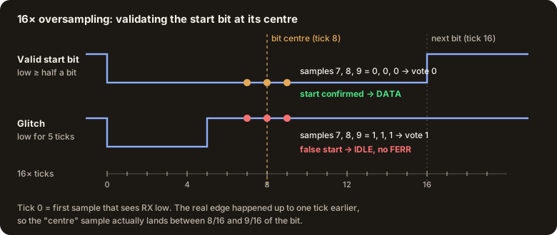
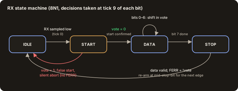
When the line is idle (1) and a tick samples 0, the FSM moves from IDLE to START and calls that tick tick 0. Instead of immediately receiving data, it waits until the centre of the start bit, about 8 ticks later, and checks the line again:
- Still 0 → it’s a real start bit. The counter keeps running, and every following bit is sampled at its centre, 16 ticks apart.
- Back to 1 → the low pulse was a glitch. The FSM returns to IDLE silently: no character, no interrupt, no framing error.
This is the textbook behaviour. A start bit is only accepted if it lasts at least half a bit time, and anything shorter is treated as a spurious pulse. 16550-class UARTs list it as false-start-bit detection.
Why “tick 8” is not exactly the centre
The receiver doesn’t watch the line continuously. It only checks it once per tick, so it never sees exactly when the falling edge happened. All it knows is that the edge came somewhere between the last high sample (tick −1) and the first low sample (tick 0):
                 real edge happened somewhere in here
                            ◄──────►
RX line    ‾‾‾‾‾‾‾‾‾‾‾‾‾‾‾‾‾‾‾‾‾‾╲______________________________ ...
samples        1         1       ╎   0         0      ...      0
             tick −2   tick −1   ╎ tick 0    tick 1   ...   tick 8
The receiver then counts 8 ticks from tick 0, but the bit really started at the edge:
- Edge just before tick 0: tick 8 is 8 ticks after the edge, which is 8/16 = 50 % of the bit, the true centre.
- Edge just after tick −1: tick 8 is almost 9 ticks after the edge, which is 9/16 ≈ 56 % of the bit.
So the centre sample is never early, but can be up to 1 tick (1/16 bit = 6.25 %) late. At 115200 baud that is up to about 0.54 µs. The receiver can’t remove this error because it never saw the real edge, and only a higher oversampling rate makes it smaller (16× is better than 8×). This lateness uses up part of the receiver’s safety margin, which is why it appears again in the clock-tolerance budget in section 6.
4. Majority voting: don’t trust a single sample
A single sample at tick 8 can be fooled by one noisy tick. Higher-reliability UART IP (common in automotive and industrial MCUs) samples three ticks around the centre, 7, 8 and 9 in 0-based counting, and takes a 2-of-3 majority:
bit_value = (S7 · S8) + (S8 · S9) + (S7 · S9)        // 2-of-3 majority
noise     = NOT (S7 = S8 = S9)                       // samples disagree
The vote produces two separate outputs, which answer two different questions:
- Bit value (majority): “what is the bit?” Whatever at least 2 of the 3 samples say.
- Noise flag (NF): “was the reading clean?” NF is set whenever the 3 samples are not all the same, even if the majority still produced the right value.
| S7 | S8 | S9 | Bit value (2-of-3 majority) | All 3 agree? | Noise flag (NF) | What probably happened |
|---|---|---|---|---|---|---|
| 0 | 0 | 0 | 0 | yes | 0 | Clean 0 |
| 0 | 0 | 1 | 0 | no | 1 | Late glitch, or the next bit arriving early (clock drift) |
| 0 | 1 | 0 | 0 | no | 1 | 1-tick spike in the middle; the vote recovers 0 |
| 1 | 0 | 0 | 0 | no | 1 | Early glitch, or this bit started late |
| 0 | 1 | 1 | 1 | no | 1 | Early glitch, or this bit started late |
| 1 | 0 | 1 | 1 | no | 1 | 1-tick dip in the middle; the vote recovers 1 |
| 1 | 1 | 0 | 1 | no | 1 | Late glitch, or the next bit arriving early (clock drift) |
| 1 | 1 | 1 | 1 | yes | 0 | Clean 1 |
Think of three judges. In the 0 1 0 row, two judges say 0, so the verdict is 0, which is
correct because the vote fixed the bad middle sample. But one judge disagreed, which means
something disturbed the line while it was being sampled. The receiver keeps the correct value
and sets NF as a warning. In the 1 1 1 row all three agree, so there is nothing to warn
about.
So NF is a warning, not an error. The data is usually still correct, but a rising NF count tells you the line is getting noisy (or the baud rates are drifting apart) before real data errors start.
The same vote is applied to the start bit, every data bit, and the stop bit.
A real-world example, STM32 USART (ST reference manual RM0360):
- Start bit: detected from the sequence
1 1 1 0 X 0 X 0 X 0 0 0 0. It checks samples 3, 5, 7 and 8, 9, 10 (counted from 1). If all six are 0, the start bit is confirmed. - Noise flag: if only 2 of 3 are 0 in either group, the start bit is still accepted but the noise flag (NF) is set.
- Silent abort: otherwise the receiver “returns to the idle state (no flag is set)”.
- Data bits: sampled by majority vote of the three centre samples, and the noise flag
(NF) is set whenever they disagree. An
ONEBIToption switches to a single centre sample, which gives more clock tolerance but no noise detection.
ST’s 8th–10th samples (counted from 1) are the same three ticks as 7–9 counted from 0. When you compare designs, always check which counting convention the documentation uses.
5. Which glitches are rejected? (the part most tests get wrong)
Let W be the width of a single clean low pulse on an idle line, and T one 16× tick.
| Pulse width W | Result | Why |
|---|---|---|
| W < T | Usually missed completely | It can fall between two samples |
| T ≤ W ≤ 8T | Always rejected (silent) | Ticks 8 and 9 already see the line high again, so the vote is 1 (tick 7 may still read low when W > 7T) |
| 8T < W < 9T | Either, depending on clock phase | Tick 8 lands just before or just after the pulse ends |
| W ≥ 9T | Always accepted as a start bit | Ticks 7 and 8 are both low |
Two things here often surprise people:
- Majority voting doesn’t move this boundary for a single clean pulse. If tick 8 is low, tick 7 is low too, so 2-of-3 is reached at the same point. Majority voting protects against a short high spike inside a genuine bit, not against a longer low glitch.
- A pulse longer than half a bit but shorter than a full bit is not an error. The start bit is confirmed, the following data bits all read 1, and the stop bit is high. The receiver delivers a valid character, typically 0xFF for 8N1 with no parity, with no framing error. Only parity, if enabled, or a higher-level checksum will catch it.
6. Stop bit, framing error, and how much clock error you can tolerate
Every subsequent bit is sampled at the centre: data bit n at about (1.5 + n) × Tbit after the start edge, and the stop bit at about 9.5 × Tbit for 8N1. If the stop bit reads 0, the receiver raises a framing error (FERR). So:
- False start → silent rejection (back to IDLE, no flag).
- Bad stop bit → FERR (frame delivered with an error flag).
After sampling the stop bit, the FSM goes back to IDLE immediately (mid-stop-bit), so it is ready for the next falling edge even if the transmitter’s stop bit is slightly short. One caveat: after a framing error the line may still be low (for example a break). Many UARTs therefore resynchronise carefully. For example, the TI TL16C550C datasheet says it treats the framing error as the next start bit and “samples this start bit twice” before accepting data.
Clock tolerance. Because the receiver re-aligns only on the start edge, any baud-rate mismatch accumulates bit by bit. The last sample must still fall inside the stop bit:
allowed total error  ≈  (0.5 − k / N) / L

N = oversampling (16 or 8)
k = 1 for a single centre sample
k = 2 for a 3-sample majority (wider sampling window)
L = frame length in bits (10 for 8N1)
This reproduces ST’s published receiver tolerance figures for 8-bit frames (RM0360, Table 89):
| Oversampling | Majority vote (3 samples) | Single sample |
|---|---|---|
| 16× | (0.5 − 2/16) / 10 = 3.75 % | (0.5 − 1/16) / 10 = 4.375 % |
| 8× | (0.5 − 2/8) / 10 = 2.50 % | (0.5 − 1/8) / 10 = 3.75 % |
This is the total budget. It must cover transmitter clock error, receiver clock error, baud-rate quantisation (divider rounding), and edge distortion on the line. A common rule of thumb is to keep each side within about half of it.
7. Validation checklist
For RTL verification and post-silicon validation of a UART receiver:
- Glitch-width sweep on an idle line. Inject single low pulses from 1 T to 16 T in small
steps, at many phase offsets relative to the sample clock.
- Expect: ≤ 8 T rejected (FSM back in IDLE, no RX interrupt, FIFO level unchanged, no framing error (FERR) or noise flag (NF)); between 8 T and 9 T may go either way, so don’t fail the test there; ≥ 9 T accepted as a character (0xFF for 8N1).
- Also check: the behaviour matches your IP’s documented sampling points.
- Spike inside a valid bit. Flip the line for 1 T exactly at the voting window (ticks 7, 8
or 9) of a start, data or stop bit.
- Expect: correct data plus the noise flag (NF). A 2 T spike across two voting samples will corrupt that bit, which proves the window is where you think it is.
- Error classification.
- False start → silent, no flag.
- Low stop bit → FERR, with the data still delivered.
- Line held low for longer than a frame → break indication, not a stream of framing errors.
- Baud-rate tolerance sweep. Offset the transmitter by ± 0.5 % steps until errors appear.
- Expect: the failure point is close to the documented tolerance (3.75 % for 16× with a majority vote, per the ST table above), minus your divider’s rounding error.
- Back-to-back frames with minimum stop length. Make sure the receiver re-arms at the middle of the stop bit and never misses the next start edge.
- Clock-domain crossing (CDC) and reset value of the RX synchroniser.
- Why: the RX pin comes from another device, so it can change at any moment relative to the receiver’s clock. If a flip-flop captures it exactly while it is changing, the flip-flop can go metastable (briefly neither a clean 0 nor a clean 1). The 2-flop synchroniser from section 1 gives it time to settle.
- Check (RTL): run a CDC lint tool (for example Questa CDC, Spyglass CDC or Conformal CDC) and confirm that no logic uses the raw pin. Only the synchronised signal may feed the edge detector and the FSM.
- Check (reset): the synchroniser flops must reset to 1 (the idle level). If they reset to 0, the receiver sees a fake falling edge right after every reset. A receiver with the half-bit check rejects it silently, but one without it (or with any other start-detection bug) delivers a garbage byte. Don’t rely on the start check to hide a reset bug.
- Check (silicon): apply resets while the line is idle and confirm that no character, interrupt or error flag appears.
- Low-power wake-up. If the UART can wake the device on RX activity, verify that a rejected glitch doesn’t leave the system awake or raise a spurious wake interrupt.
References
- STMicroelectronics, RM0360 reference manual (STM32F030/F070), Rev 5: USART receiver, start bit detection, noise error, framing error, receiver tolerance (Tables 89–90).
- Texas Instruments, TL16C550C asynchronous communications element datasheet (SLLS177I): 16× reference clock, false-start-bit detection, resynchronisation after a framing error.
- Maxim Integrated (now Analog Devices), Application Note 2141, Determining Clock Accuracy Requirements for UART Communications (2003).
- Wikipedia, Universal asynchronous receiver-transmitter: Receiver.
Every UART IP documents its own sampling points and flags. Always check your device’s reference manual before writing pass/fail limits.
Stay in touch
Found this useful?
Follow me on LinkedIn for more posts on silicon validation, embedded systems and CPU internals.
Follow me on LinkedIn